Address
304 North Cardinal
St. Dorchester Center, MA 02124
Work Hours
Monday to Friday: 7AM - 7PM
Weekend: 10AM - 5PM
Address
304 North Cardinal
St. Dorchester Center, MA 02124
Work Hours
Monday to Friday: 7AM - 7PM
Weekend: 10AM - 5PM
Gigabyte ga-h61m-d1 mainboard triggers power down repair
Motherboard model: Gigabyte ga-h61m-d1 Rev: 1.0
Fault phenomenon: main board switch auto power off
Maintenance process:
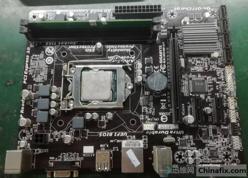
Gigabyte ga-h61m-d1 mainboard triggers power down repair Figure 1.
A gigabyte ga-h61m-d1 motherboard, the fault is power on, turn to stop,switch auto power off,switch again, no CPU VCC measured.
First test several VCC and signals before the CPU VCC: according to H61 timing memory bridge vccpll VTT vccsa, etc
The first VCC: the memory is 1.5V. Generally, 1.5V is normal on the Inductor next to the memory socket.
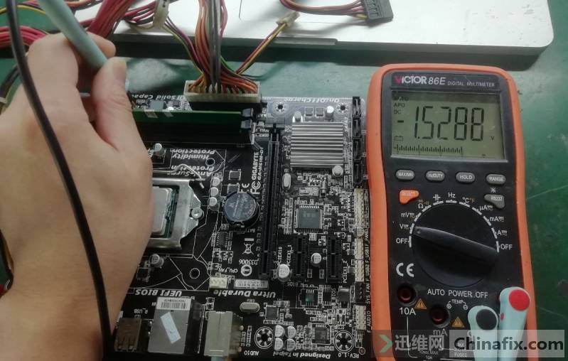
Gigabyte ga-h61m-d1 mainboard triggers power down repair Figure 2.
The second VCC: Bridge 1.05v, MOS near the bridge measured 1.05v normal.
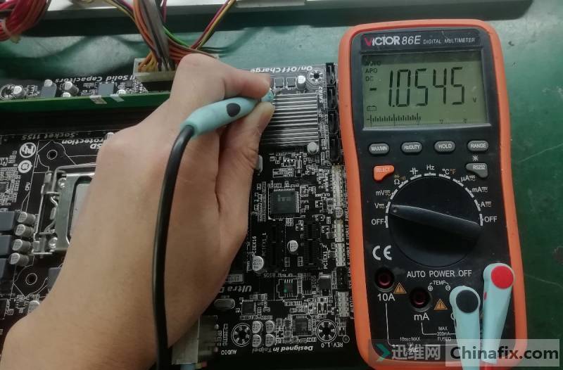
Gigabyte ga-h61m-d1 mainboard triggers power down repair Figure 3.
The third VCC: phase locked loop VCC vccpll 1.8V, generally measured between the bridge and the CPU socket between the MOSFET is normal.
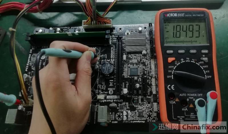
Gigabyte ga-h61m-d1 mainboard triggers power down repair Figure 4.
The fourth VCC: bus VCC 1.05v, 1.05v between MOSFET between bridge and CPU socket is normal.
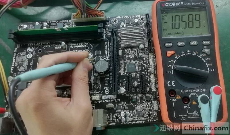
Gigabyte ga-h61m-d1 mainboard triggers power down repair Figure 5.
The fifth VCC: the system manager vccsa is 0.94v. Generally, the MOSFET between the headphone socket and the CPU socket measures 0.94v, which is also normal.
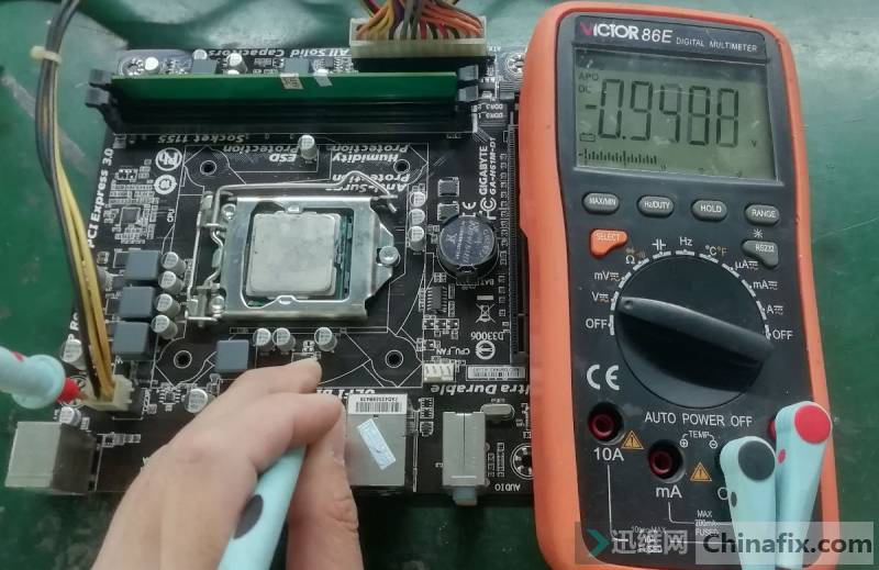
Gigabyte ga-h61m-d1 mainboard triggers power down repair Figure 5.
VCC is normal after testing, and the 67 series PG reset block diagram with poor copy is repaired on time and in sequence.
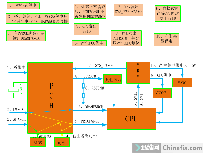
Gigabyte ga-h61m-d1 mainboard triggers power down repair Figure 6.
PCH should receive two PG (pwrok1) after VCC is normal. When the tweezers are pulled out, there is VCC in a moment.
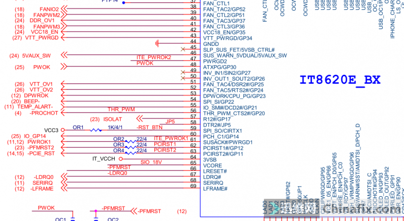
Gigabyte ga-h61m-d1 mainboard triggers power down repair Figure 7.
The pwrok1 signal of Gigabyte is normal at VCC with reference to 8728 IO, and SLP is received_S3 atxpg detected that 12 V 5 V 3.3 V was normal, and the signal was delayed.
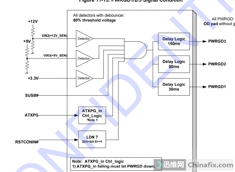
Gigabyte ga-h61m-d1 mainboard triggers power down repair Figure 8.
CLK 01 on slot a16601 is flashing.
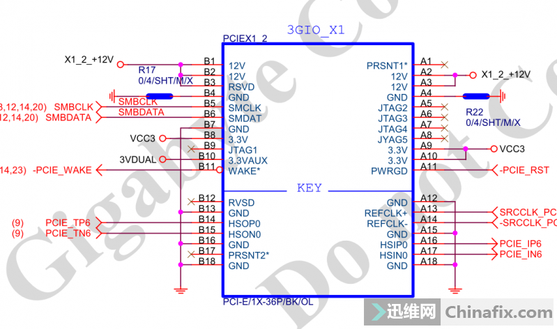
Gigabyte ga-h61m-d1 mainboard triggers power down repair Figure 9.
Open the drawing to test whether the VCC of VRM is turned on normally. If you change the power management chip, the CPU VCC still doesn’t come out. It’s the same to change another one.
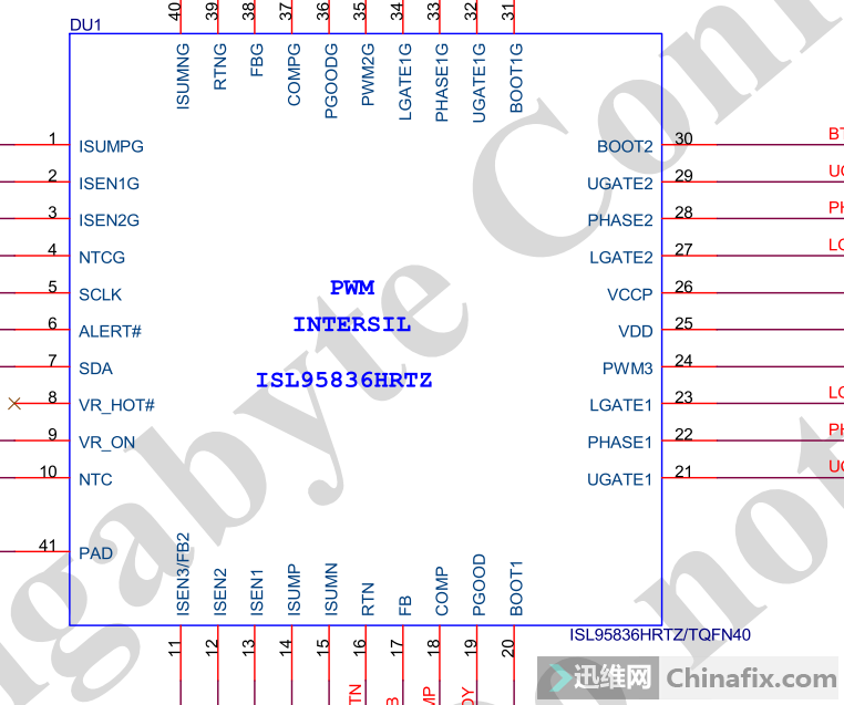
Gigabyte ga-h61m-d1 mainboard triggers power down repair Figure 10.
Turn on the oscilloscope and test VCC again. A problem is found in the VCC unstable bus.
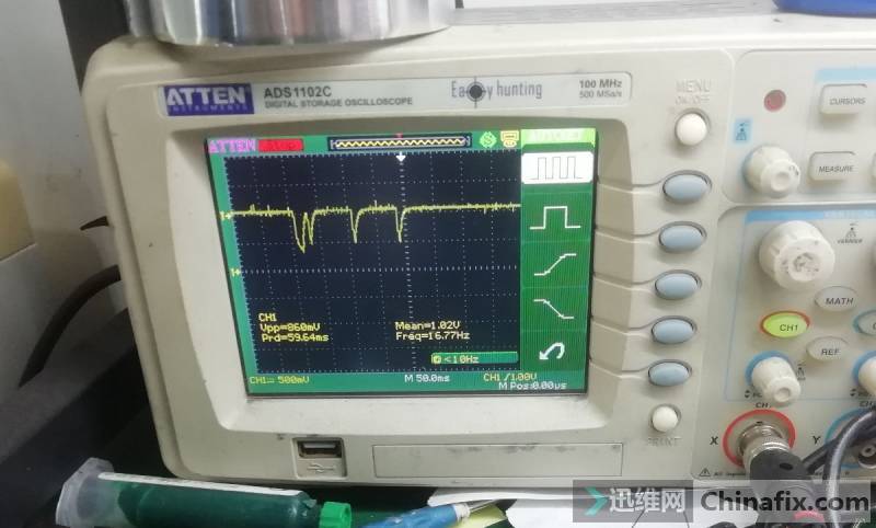
Gigabyte ga-h61m-d1 mainboard triggers power down repair Figure 11.
Jijia’s voltage divider resistance is broken more, and it is found that it is caused by VREF unstable of comparator 5 pin.
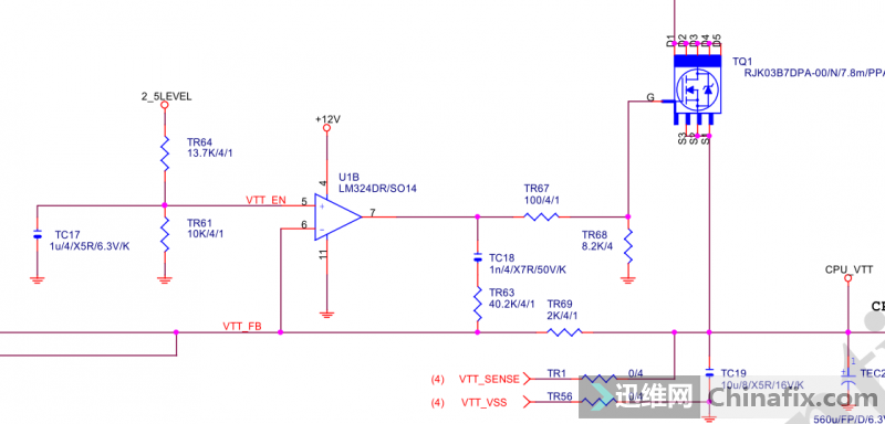
Gigabyte ga-h61m-d1 mainboard triggers power down repair Figure 12.
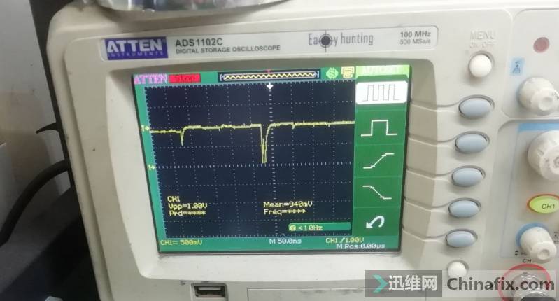
Gigabyte ga-h61m-d1 mainboard triggers power down repair Figure 13.
Repair after replacement of voltage divider resistor.Connected to monitor,Normally booting up.
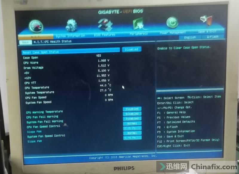
Gigabyte ga-h61m-d1 mainboard triggers power down repair Figure 14.